- 您现在的位置:买卖IC网 > Sheet目录1999 > ICS87974CYILF (IDT, Integrated Device Technology Inc)IC CLK GEN LVCMOS/LVTTL 52-LQFP
87974CYI
www.idt.com
REV. E JULY 26, 2010
1
ICS87974I
LOW SKEW, 1-TO-15,
LVCMOS/LVTTL CLOCK GENERATOR
GENERAL DESCRIPTION
The ICS87974I is a low skew, low jitter 1-to-15 LVCMOS/
LVTTL Clock Generator/Zero Delay Buffer. The device has
a fully integrated PLL and three banks whose divider ratios
can be independently controlled, providing output
frequency relationships of 1:1, 2:1, 3:1, 3:2, 3:2:1. In
addition, the external feedback connection provides for a
wide selection of output-to-input frequency ratios. The CLK0
and CLK1 pins allow for redundant clocking on the input
and dynamically switching the PLL between two clock
sources.
Guaranteed low jitter and output skew characteristics make
the ICS87974I ideal for those applications demanding well
defined performance and repeatability.
FEATURES
Fully integrated PLL
Fifteen single ended 3.3V LVCMOS/LVTTL outputs
Two LVCMOS/LVTTL clock inputs for redundant clock
applications
CLK0 and CLK1 accepts the following input levels:
LVCMOS/LVTTL
Output frequency range: 8.33MHz to 125MHz
VCO range: 200MHz to 500MHz
External feedback for ”zero delay” clock regeneration
Cycle-to-cycle jitter: ±100ps (typical)
Output skew: 350ps (maximum)
3.3V operating supply
-40°C to 85°C ambient operating temperature
Available in both standard and lead-free RoHS-compliant
packages
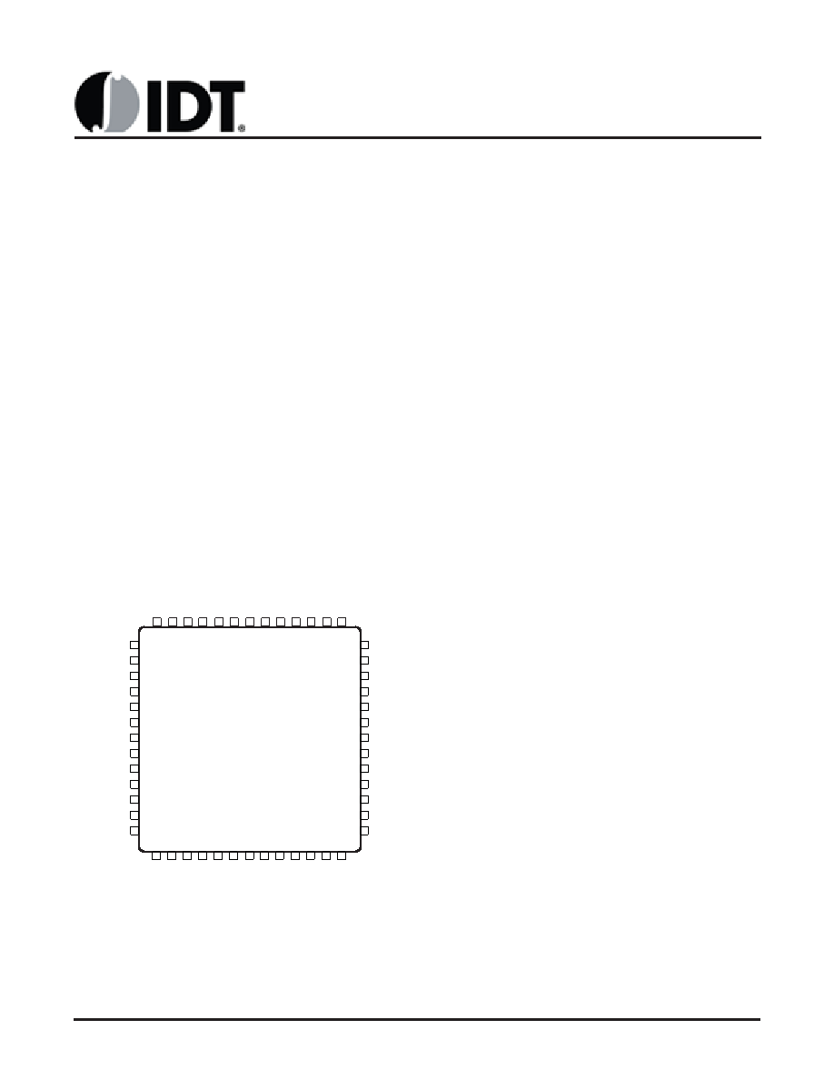
PIN ASSIGNMENT
V
DDOA
QA0
GND
QA1
V
DDOA
QA2
FB_SEL1
GND
QA3
V
DDOA
QA4
GND
FB_SEL0
GND
nMR/OE
CLK_EN
SEL_B
SEL_C
PLL_SEL
SEL_A
CLK_SEL
CLK0
CLK1
nc
VDD
VDDA
1
2
3
4
5
6
7
8
9
10
11
12
13
14 15 16 17 18 19 20 21 22 23 24 25 26
39
38
37
36
35
34
33
32
31
30
29
28
27
52 51 50 49 48 47 46 45 44 43 42 41 40
GND
QB1
VDDOB
QB2
GND
QB3
VDDOB
QB4
FB_IN
GND
QFB
VDDOFB
nc
QB0
V
DDOB
nc
GND
QC3
V
DDOC
QC2
GND
QC1
V
DDOC
QC0
GND
VCO_SEL
ICS87974I
52-Lead LQFP
10mm x 10mm x 1.4mm package body
Y package
Top View
发布紧急采购,3分钟左右您将得到回复。
相关PDF资料
ICS894D115AGI-04LF
IC CLK/DATA RECOVERY 20-TSSOP
ICS894D115BGI-01LF
IC CLK/DATA RECOVERY 20-TSSOP
ICS9112AM-17LF
IC BUFFER HI PERFORMANCE 16-SOIC
ICS91305AMILF
IC CLOCK DRIVER LO JITTER 8-SOIC
ICS91305AMLF
IC CLOCK DRIVER LO JITTER 8-SOIC
ICS91309AGILF
IC CLK BUFFER ZD PLL 16TSSOP
ICS9161A-01CW16T
IC FREQUENCY GENERATOR 16-SOIC
ICS91730AMLF
IC CLOCK GENERATOR LOW EMI 8SOIC
相关代理商/技术参数
ICS87974CYILFT
功能描述:IC CLOCK GEN 1-15 PLL 52-LQFP RoHS:是 类别:集成电路 (IC) >> 时钟/计时 - 时钟发生器,PLL,频率合成器 系列:HiPerClockS™ 标准包装:1,000 系列:- 类型:时钟/频率合成器,扇出分配 PLL:- 输入:- 输出:- 电路数:- 比率 - 输入:输出:- 差分 - 输入:输出:- 频率 - 最大:- 除法器/乘法器:- 电源电压:- 工作温度:- 安装类型:表面贴装 封装/外壳:56-VFQFN 裸露焊盘 供应商设备封装:56-VFQFP-EP(8x8) 包装:带卷 (TR) 其它名称:844S012AKI-01LFT
ICS879893AYILF
功能描述:IC CLK GEN LVCMOS/LVTTL 48-LQFP RoHS:是 类别:集成电路 (IC) >> 时钟/计时 - 时钟发生器,PLL,频率合成器 系列:HiPerClockS™ 标准包装:1,000 系列:- 类型:时钟/频率合成器,扇出分配 PLL:- 输入:- 输出:- 电路数:- 比率 - 输入:输出:- 差分 - 输入:输出:- 频率 - 最大:- 除法器/乘法器:- 电源电压:- 工作温度:- 安装类型:表面贴装 封装/外壳:56-VFQFN 裸露焊盘 供应商设备封装:56-VFQFP-EP(8x8) 包装:带卷 (TR) 其它名称:844S012AKI-01LFT
ICS879893AYILFT
功能描述:IC CLK GEN LVCMOS/LVTTL 48-LQFP RoHS:是 类别:集成电路 (IC) >> 时钟/计时 - 时钟发生器,PLL,频率合成器 系列:HiPerClockS™ 标准包装:1,000 系列:- 类型:时钟/频率合成器,扇出分配 PLL:- 输入:- 输出:- 电路数:- 比率 - 输入:输出:- 差分 - 输入:输出:- 频率 - 最大:- 除法器/乘法器:- 电源电压:- 工作温度:- 安装类型:表面贴装 封装/外壳:56-VFQFN 裸露焊盘 供应商设备封装:56-VFQFP-EP(8x8) 包装:带卷 (TR) 其它名称:844S012AKI-01LFT
ICS87993AYILF
功能描述:IC PLL CLK DRIVER 1-5 32-LQFP RoHS:是 类别:集成电路 (IC) >> 时钟/计时 - 时钟发生器,PLL,频率合成器 系列:HiPerClockS™ 标准包装:1,000 系列:- 类型:时钟/频率合成器,扇出分配 PLL:- 输入:- 输出:- 电路数:- 比率 - 输入:输出:- 差分 - 输入:输出:- 频率 - 最大:- 除法器/乘法器:- 电源电压:- 工作温度:- 安装类型:表面贴装 封装/外壳:56-VFQFN 裸露焊盘 供应商设备封装:56-VFQFP-EP(8x8) 包装:带卷 (TR) 其它名称:844S012AKI-01LFT
ICS87993AYILFT
功能描述:IC PLL CLK DRIVER 1-5 32-LQFP RoHS:是 类别:集成电路 (IC) >> 时钟/计时 - 时钟发生器,PLL,频率合成器 系列:HiPerClockS™ 标准包装:1,000 系列:- 类型:时钟/频率合成器,扇出分配 PLL:- 输入:- 输出:- 电路数:- 比率 - 输入:输出:- 差分 - 输入:输出:- 频率 - 最大:- 除法器/乘法器:- 电源电压:- 工作温度:- 安装类型:表面贴装 封装/外壳:56-VFQFN 裸露焊盘 供应商设备封装:56-VFQFP-EP(8x8) 包装:带卷 (TR) 其它名称:844S012AKI-01LFT
ICS889474AKLF
功能描述:IC CLK BUFFER MUX 2:2 24-VFQFPN RoHS:是 类别:集成电路 (IC) >> 时钟/计时 - 时钟缓冲器,驱动器 系列:HiPerClockS™ 标准包装:74 系列:- 类型:扇出缓冲器(分配) 电路数:1 比率 - 输入:输出:1:10 差分 - 输入:输出:是/是 输入:HCSL, LVCMOS, LVDS, LVPECL, LVTTL 输出:HCSL,LVDS 频率 - 最大:400MHz 电源电压:3 V ~ 3.6 V 工作温度:-40°C ~ 85°C 安装类型:表面贴装 封装/外壳:32-VFQFN 裸露焊盘 供应商设备封装:32-QFN(5x5) 包装:管件
ICS889474AKLFT
功能描述:IC CLK BUFFER MUX 2:2 24-VFQFPN RoHS:是 类别:集成电路 (IC) >> 时钟/计时 - 时钟缓冲器,驱动器 系列:HiPerClockS™ 标准包装:74 系列:- 类型:扇出缓冲器(分配) 电路数:1 比率 - 输入:输出:1:10 差分 - 输入:输出:是/是 输入:HCSL, LVCMOS, LVDS, LVPECL, LVTTL 输出:HCSL,LVDS 频率 - 最大:400MHz 电源电压:3 V ~ 3.6 V 工作温度:-40°C ~ 85°C 安装类型:表面贴装 封装/外壳:32-VFQFN 裸露焊盘 供应商设备封装:32-QFN(5x5) 包装:管件
ICS889831AKLF
功能描述:IC CLK BUFF 1:4 2.1GHZ 16-VFQFPN RoHS:是 类别:集成电路 (IC) >> 时钟/计时 - 时钟缓冲器,驱动器 系列:HiPerClockS™ 标准包装:1 系列:HiPerClockS™ 类型:扇出缓冲器(分配),多路复用器 电路数:1 比率 - 输入:输出:2:18 差分 - 输入:输出:是/无 输入:CML,LVCMOS,LVPECL,LVTTL,SSTL 输出:LVCMOS,LVTTL 频率 - 最大:250MHz 电源电压:2.375 V ~ 3.465 V 工作温度:0°C ~ 70°C 安装类型:表面贴装 封装/外壳:32-LQFP 供应商设备封装:32-TQFP(7x7) 包装:- 其它名称:800-1923-6